Product Description
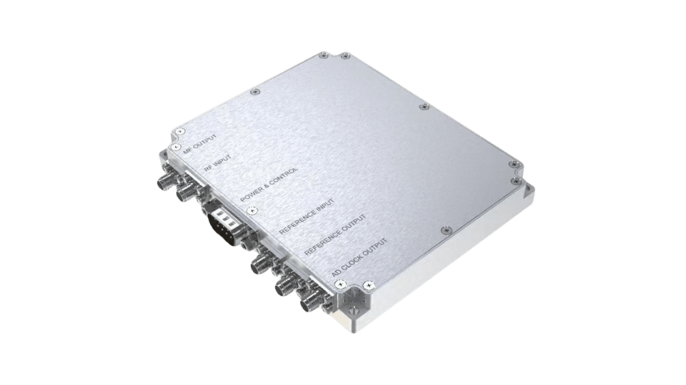
20MHz to 40GHz RF Frequency Converter Module VFC-20-40000-320
The VFC-20-40000-320 Wideband Frequency Converter Module is a high-performance RF device, specifically designed for precise frequency conversion and efficient signal processing, with a wide frequency range from 20MHz to 8GHz. It is widely used in RF testing, electronic warfare, radar systems, communication equipment, and research fields, particularly in applications that require high signal quality and conversion accuracy. Whether for high-frequency signal reception, frequency conversion, or signal processing in complex systems, this module provides a reliable and efficient solution.
Technical Specifications
- Receive Frequency Range:
- 20MHz – 8GHz (Port A)
- 8GHz – 40GHz (Port B)
- Tuning Resolution: 10kHz
- Frequency Switching Time: ≤100μs
- Frequency Accuracy: ≤0.1ppm (over full temperature range)
- Phase Noise:
- ≤-120dBc/Hz at 10kHz offset @ 1GHz
- ≤-108dBc/Hz at 10kHz offset @ 8GHz
- ≤-102dBc/Hz at 10kHz offset @ 18GHz
- ≤-98dBc/Hz at 10kHz offset @ 40GHz
- Frequency Converter Modes: Normal Mode, Low Distortion Mode, Low Noise Mode
- Noise Figure:
- ≤9dB (20MHz – 3.6GHz)
- ≤11dB (3.6GHz – 8GHz)
- ≤13dB (8GHz – 18GHz)
- ≤15dB (18GHz – 40GHz) in Low Noise Mode
- Link Gain:
- 45±2dB (Low Noise Mode)
- 30±2dB (Normal Mode)
- 10±2dB (Low Distortion Mode)
- Intermediate Frequency (IF) Frequency:
- Wideband: 614.4MHz
- Narrowband: 638MHz
- Intermediate Frequency Bandwidth:
- Wideband 1: 320MHz
- Wideband 2: 80MHz
- Narrowband 1: 4MHz
- Intermediate Frequency Filter Rectangular Coefficient: ≤1.5 (BW-60dB/BW-3dB) in Wideband 1
- RF Attenuation: 0–30dB (1dB steps)
- IF Attenuation: 0–30dB (1dB steps)
- IF Suppression: ≥90dB (typical)
- Image Suppression: ≥90dB (typical)
- Input 2nd Order Intercept Point: ≥60dBm (typical) in Low Distortion Mode
- Input 3rd Order Intercept Point: ≥20dBm (typical) in Low Distortion Mode
- Output 1dB Compression Point: ≥15dBm
- Burnout Power: 30dBm
- Impedance: 50Ω
- Internal Spurious Signals: ≤-110dBm (referenced to input, typical)
- Frequency Fine Tuning: Supported
- AD Clock Output: Frequency: 819.2MHz, Output Power: 4±2dBm
- Built-in Reference Clock: Frequency: 100MHz, Automatic switching between internal and external reference clocks
- External Reference Clock Input: Supports 100MHz or 10MHz
- Intermediate Frequency Output In-Band Variation: ≤3dB (typical)
Initialization State
- Frequency Conversion Module Tuning Frequency: 500MHz
- Frequency Conversion Module RF Attenuation: 10dB
- Frequency Conversion Module Intermediate Frequency Attenuation: 20dB
- Frequency Conversion Module Operating Mode: Normal Operating Mode
- Frequency Conversion Module Intermediate Frequency Bandwidth: 160MHz
- SPI Interface Operating State: Waiting to receive external control data
Other
- Operating Temperature: -40°C ~ +60°C
- Storage Temperature: -58°C ~ +85°C
- Power and Control Interface: J30J-9ZKP
- Power Supply: DC: 12V (±5%) I ≤ 1.5A
- RF Interface: SMA-K,2.92-K
- Dimensions: 120mm × 100mm × 32mm (Tolerance ±0.2mm, excluding connector size)
- Weight: ≤1.2kg
Low-Frequency Interface Definition(Pin Definition of Connector J30J-9ZKP)
- Pin 1: SCK (Synchronous Clock Signal)
- Pin 2: SDI (Input Data Signal)
- Pin 3: /SS (Input Active Signal)
- Pin 4: SDO (Output Data Signal)
- Pin 5: NC (No Connection)
- Pin 6: +12V Input
- Pin 7: +12V Input
- Pin 8: GND (Ground)
- Pin 9: GND (Ground)