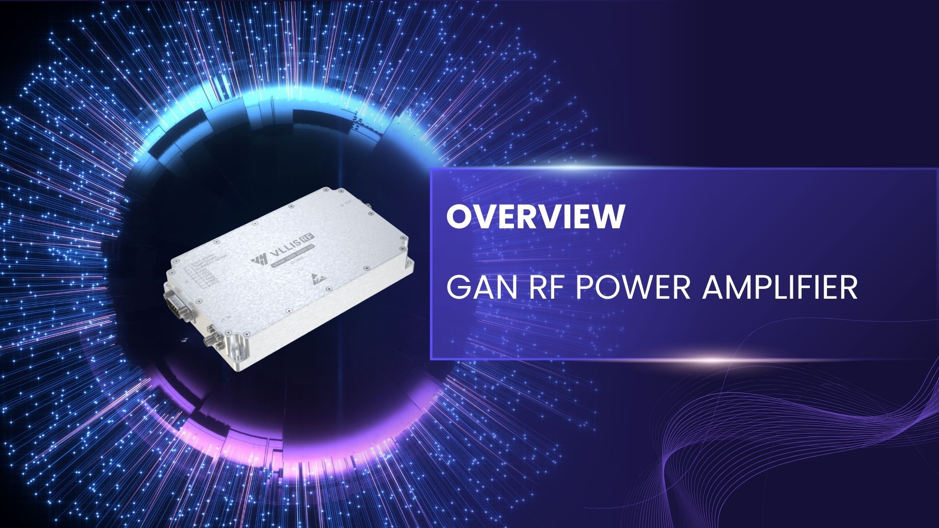
GaN RF Power Amplifiers Overview | Design, Applications, and Future Trends
Gallium Nitride (GaN) RF Power Amplifiers have revolutionized the field of high-frequency electronics by offering exceptional power density, efficiency, and bandwidth compared to traditional technologies such as silicon (Si) and gallium arsenide (GaAs). As the demand for 5G, satellite communications, radar, and defense systems continues to grow, GaN has emerged as the leading semiconductor material for RF power amplification.
What is a GaN RF Power Amplifier?
A GaN RF Power Amplifier is an electronic device that increases the amplitude of RF signals using Gallium Nitride transistors as the active component. GaN transistors exhibit high breakdown voltage, high electron mobility, and wide bandgap properties, which allow amplifiers to deliver higher power output, greater efficiency, and operation at higher frequencies compared to their silicon and GaAs counterparts.
Key Advantages of GaN
- High power density (up to 10× compared to GaAs)
- High breakdown voltage (>200 V)
- High efficiency (>70% achievable)
- Wide frequency range: HF to Ka-band and beyond
- Excellent thermal stability and reliability
Working Principles of GaN Devices
GaN belongs to the family of wide bandgap semiconductors with a bandgap of 3.4 eV, much higher than Si (1.1 eV) or GaAs (1.4 eV). This allows for higher electric fields before breakdown and enables devices with high power density and frequency performance.
HEMT Structure
Most GaN RF devices are based on High Electron Mobility Transistors (HEMTs). The 2-dimensional electron gas (2DEG) formed at the heterojunction provides high mobility and high current-carrying capability.
Equation for Drain Current
Id ≈ μn·Cgs·(W/L)·(Vgs-Vth)²
where μn is electron mobility, Cgs is gate capacitance, W/L is transistor geometry, and Vth is threshold voltage.
High Breakdown Voltage
The critical electric field of GaN is about 3.3 MV/cm, which enables high voltage operation, essential for high RF output power.
Key Performance Metrics
- Gain (dB)
- Power-Added Efficiency (PAE)
- Output Power (P1dB, Psat)
- Linearity (ACPR, IMD)
- Thermal Resistance (°C/W)
- Reliability (MTTF, degradation rates)
Design Considerations and Techniques
Impedance Matching
GaN devices typically have low input and output impedances, requiring broadband matching networks.
Biasing
Stable bias networks with temperature compensation are required for reliable operation.
Harmonic Termination
Proper load-pull optimization helps improve efficiency by managing harmonic terminations.
Thermal Management and Reliability
Thermal dissipation is a critical design factor. GaN devices operate at high power densities and require advanced packaging such as copper-molybdenum carriers, diamond heat spreaders, and advanced PCB thermal vias.
Thermal Equation
ΔT = Pdiss × RθJC
where ΔT is junction temperature rise, Pdiss is power dissipation, and RθJC is junction-to-case thermal resistance.
Linearity and Linearization
GaN amplifiers provide high efficiency but can suffer from non-linear distortion. Common techniques include:
- Doherty architecture
- Envelope tracking
- Digital predistortion (DPD)
Power Combining Techniques
- Corporate combining networks
- Spatial power combining
- Hybrid combiners
- Load-pull optimization methods
Applications
5G and Wireless Infrastructure
GaN amplifiers support massive MIMO and carrier aggregation with high efficiency.
Radar Systems
High peak power and fast switching make GaN ideal for radar transmitters.
Satellite Communication
Wideband linear amplification for Ku/Ka-band links.
Electronic Warfare
High power and broadband coverage for jamming systems.
Automotive Radar
77 GHz GaN solutions enable autonomous driving sensors.
Engineering Case Studies
Case 1: 5G Base Station PA
3.5 GHz, 200 W GaN Doherty amplifier achieving 55% efficiency.
Case 2: X-band Radar
10 GHz, 1 kW solid-state power amplifier with corporate combining.
Case 3: Ka-band SATCOM
30 GHz GaN amplifier with 40% PAE for satellite uplink.
Future Trends in GaN RF Amplifiers
- Integration with MMICs for compact modules
- Higher frequency operation up to W-band
- Monolithic GaN-on-diamond devices for thermal management
- AI-driven digital predistortion for adaptive linearization
- Wide adoption in automotive and IoT markets
Conclusion
GaN RF Power Amplifiers are redefining RF and microwave system design. Their superior efficiency, wide bandwidth, and high power density make them the technology of choice for 5G, satellite, radar, and defense applications. With ongoing advances in material science, packaging, and system integration, GaN amplifiers will continue to shape the future of high-frequency communications and electronic warfare systems.
